PCB Lamination Exposing & Etching (Revised)
Practical: PCB LAMINATION, ETCHING AND EXPOSING
Teacher: Mr. Babar
Lab: PCB LAB (ELECTRONICS DEPARTMENT)
Lamination
PCB lamination is an important process in PCB manufacturing. The Lamination sheet is basically made up of epoxy resin that is a photo sensitive material. Lamination comes in the form of a sheet that is covered by protective coverings from both sides. One of these two protective sheets is removed by the laminator itself. The other one is removed after exposing it to light. Laminator is a machine that is used for providing lamination on a PCB. Basically, it totally works like a plastic coating machine. From one side, we enter our copper plated PCB (which may be drilled initially or may not be) and then, we get the fully coated (with lamination sheet) PCB from both sides. Remember! that the temperature of working can also be set in the machine and the time for the lamination is also controlled. We used a 30 sec time for our double sided PCB. The PCB is entered and we get a fully coated PCB (coated from both sides) in our hands from the other side of the laminator.
Exposing
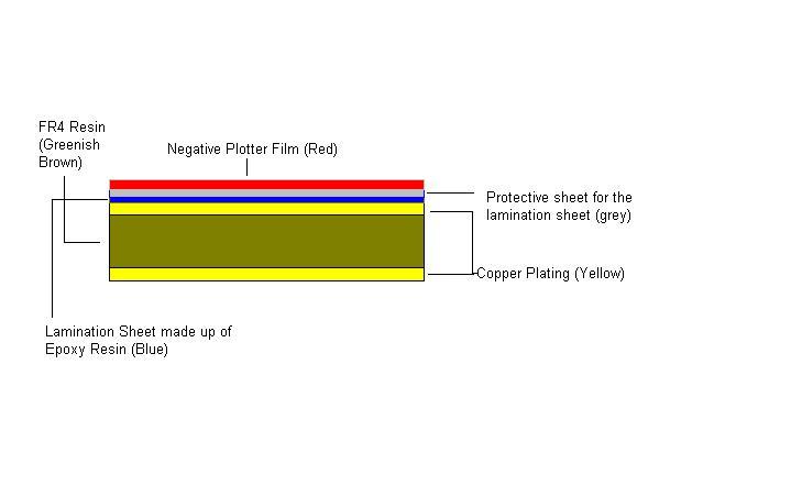
Now, after applying this lamination, we head towards another prcoess which is th exposing process. In this process we expose our PCB towards UV light. Have a look at the state of the PCB just before exposing:

My dear friends! here comes the real confusion among the students that makes them uninterested in the subject of PCB Manufacturing. The confusion that the students usually have is to know the polarity of the films we have used in this process. By polarity i mean Positive or Negative. Now that is the reason why i have revised this article in order to make you understand the right concept. But before doing that, it is required that you free up your mind from all your previous polarity concepts and then start studying below:
There are two types of Plotter Mask. One is positive and the other is negative.
The positive plotter mask has the Tracks in Black Colour. and thus wherever the tracks are present, light cannot pass through that area. Have a look at the fig below:

Now you can see, the tracks are in black color, so when light falls on such a mask, it passess through the white/transparent areas but get blocked from the black color.
Now, A Negative plotter mask has the Tracks in white/Transparent color, and thus wherever the tracks are present, light passess through them. Have a look at the fig below:

Now when the light will fall on such a plotter mask, it will pass through the areas of tracks only as they are transparent while the light will remain blocked from the remaining black area.
Now lets discuss the polarities of the Photoresist Films. Yeah! it is correct that the photoresist film is also of two types. Positive and Negative.
Now lets see what are these two types:
POSITIVE PHOTO RESIST:
when UV light falls on a positive photo resist film, the underlying material gets removed.
This thing must be kept in the mind. The Positive Photoresist will be used when you want to remove the material from those areas where the light is falling. So now quickly test yourself and answer my question :
What type of Plotter Mask would you use when using a Positive Photoresist Film?
Ans: Positive Plotter Mask
why? the reason is simple, you want to get copper remain on those areas where your sweet tracks are present and from other areas, the Cu should be removed. When you will use the Positive Plotter (which has black tracks) with a positive Photoresist film, the light will pass through those areas only which are other than the tracks. and hence the Cu will be removed from those areas which are other than the tracks. Lets discuss the chemistry of the positive Photo resist film a little. Actually when UV falls on such a film, it changes the chemical structure of the resist, as a result when you will put it in the developer in the developing process, it will become more soluble in the developer and thus washed away while developing it. But remember, those areas which are not exposed to light will not get soluble in the developer and thus will remain intact. This is you want!! that is you want your tracks areas to remain there. I think you now got it right? hahaha!!
NEGATIVE PHOTO RESIST:
when UV light falls on a negative photo resist film, the areas on which the UV light falls remain as it as while the areas on which the light does not fall, gets removed. Lets discuss the chemistry of it a little. When light falls on a negative photoresist film, it causes the resists to become polymerized and thus more difficult to dissolve. Thus the exposed areas remain intact during developing while the unexposed areas get removed during the developing process.
This time, you probably have guessed yourself the correct plotter mask for such film. It is right!
The plotter mask would be negative (containing tracks as transparent) so it will allow the light to pass through the tracks areas through the negative photo resist and as a result the track areas will get more difficult to dissolve and will remain as it as. The light blocked areas will get removed. Just remember the following formula:
If you want to get Cu on Tracks only as an output, you have to use
Positive Plotter Mask with Positive Photoresiste Film
Negative Plotter Mask with Negative Photoresist Film
I hope that you understand that. Even then you should have a look at the fig below:

Now! my dear friends! from now you should not have any confusion regarding this polarity issue.
If you have cleared your confusions regarding polarity, it would be better to start exposing.So, we will place it in the exposure box, Which contains tubelights on both sides that emits UV light. The box looks like a Photostate machine. The time duration is again 30 sec which can be set easily on the exposing machine. 
After exposing, you will see that your image is now transferred on the PCB. It is important to understand what actually happens during exposing. The areas where UV light passes through remains unfixed while the area that remains hidden from light is fixed. As we have applied the negative plotter mask above, so it will allow light in the areas other than the tracks.
Developing
Now we are left with fixed and unfixed copper and epoxy. Now remove the plotter mask as well as the remaining protective cover of the lamination sheet which was left by the laminator. And put this PCB in the developer. Basically, developer removes the unfixed areas of epoxy. The time duration is 2 minutes here. Remember that the developer will have no effect on the fixed area of epoxy and copper.
Etching
After developing, what we are left with is the unfixed copper and the fixed copper. Surely, we would never like to remove the fixed copper area. Now our target is to remove the unfixed areas of copper. For this we use the process of etching. In etching Ferric chloride is used. It removes the unfixed areas of copper and has no effect on the fixed areas. The time for normal etching is 10 min. This can be large if your chemical is older or if your copper area is greater.
CAUSTIC Operation
After etching, what we are left with, is simply the copper tracks with fixed epoxy on their top. Now, we want to remove this fixed epoxy as well. For this we will introduce our PCB in the CAUSTIC. This caustic will remove this fixed epoxy from the top of our copper tracks as well as it will also open the holes which were covered due to this fixed epoxy.
Protection from Oxidation
After this, we will get our PCB in almost a final stage, It will be very shiny and beautiful. But it will not remain shiny and beautiful if we will not protect it from oxidation which is very much possible in open air. So we will apply a simple manual coating of LACKERS, a chemical which once coated can protect the PCB from oxidation for about a year.
Now our PCB is in our hand, apply solder mask layer and then silk screen and enjoy ur electronic creation…..
posted by SB @ 5:49 AM
![]()


